


Our Laboratories
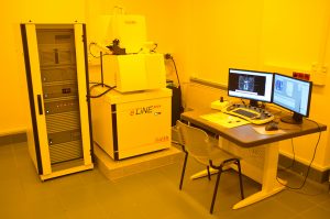
- High-resolution electron-beam lithography e-Line Plus (Raith)
Equipment for the production of nanoelectronics devices and nanocontacts with minimal width of ~50 nm (after lift – off). SEM studies of sample surfaces (InLens and SE detectors, up to 30 kV), 3D imaging
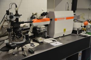
- Raman system integrated with AFM microscope
Renishaw inVia Raman spectrometer with several excitement lines (514, 633, 1064 nm) with a temperature option, suited for 2D materials and composite studies
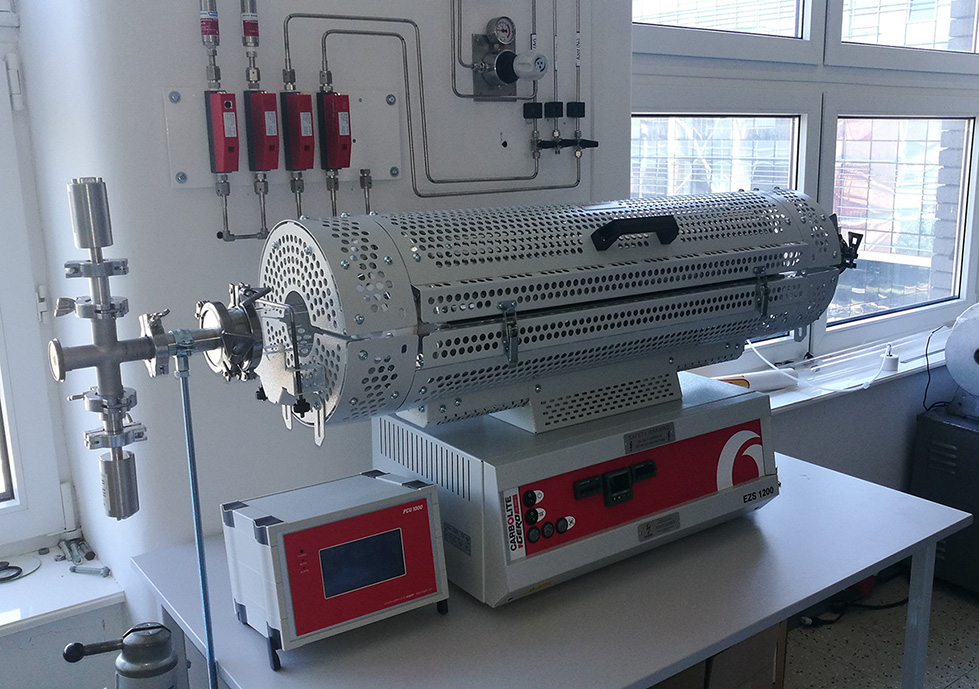
- Carbolite vacuum system for 2D materials growth
Three-zone system for CVD growth of 2D materials (e.g. graphene, MoS2 , WS2 , hBN)
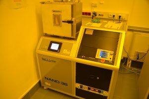
- Thermal evaporation system – Lesker Nano 36
Thermal evaporation of metallic thin films (e.g. Au, Cr, Cr, Pd, Pt, Al, Co) and oxdies (e.g. Al 2 O 3 ). Thickness deviation 0.1 nm, maximum surface area – 6”
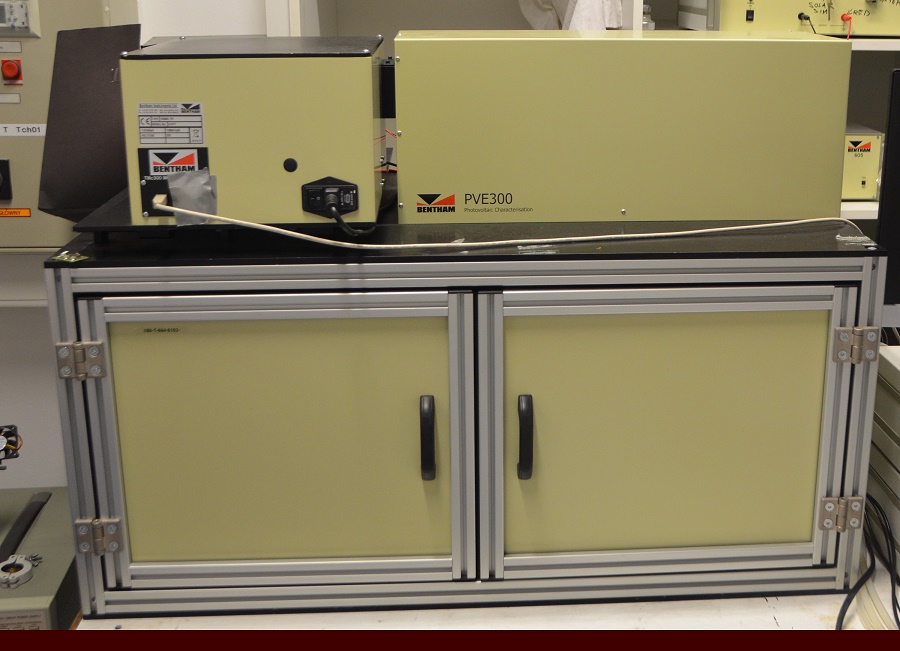
- PVE300 Bentham – device for measuring photovoltaic paramters
Spectral range – 350-1800 nm, resolution 1 – 2 nm. Measurements of transmittance, reflectance and absorbance in the function of wavelength. Integrating sphere. Measurements of solar cell quantum efficiency. Sun simulator.
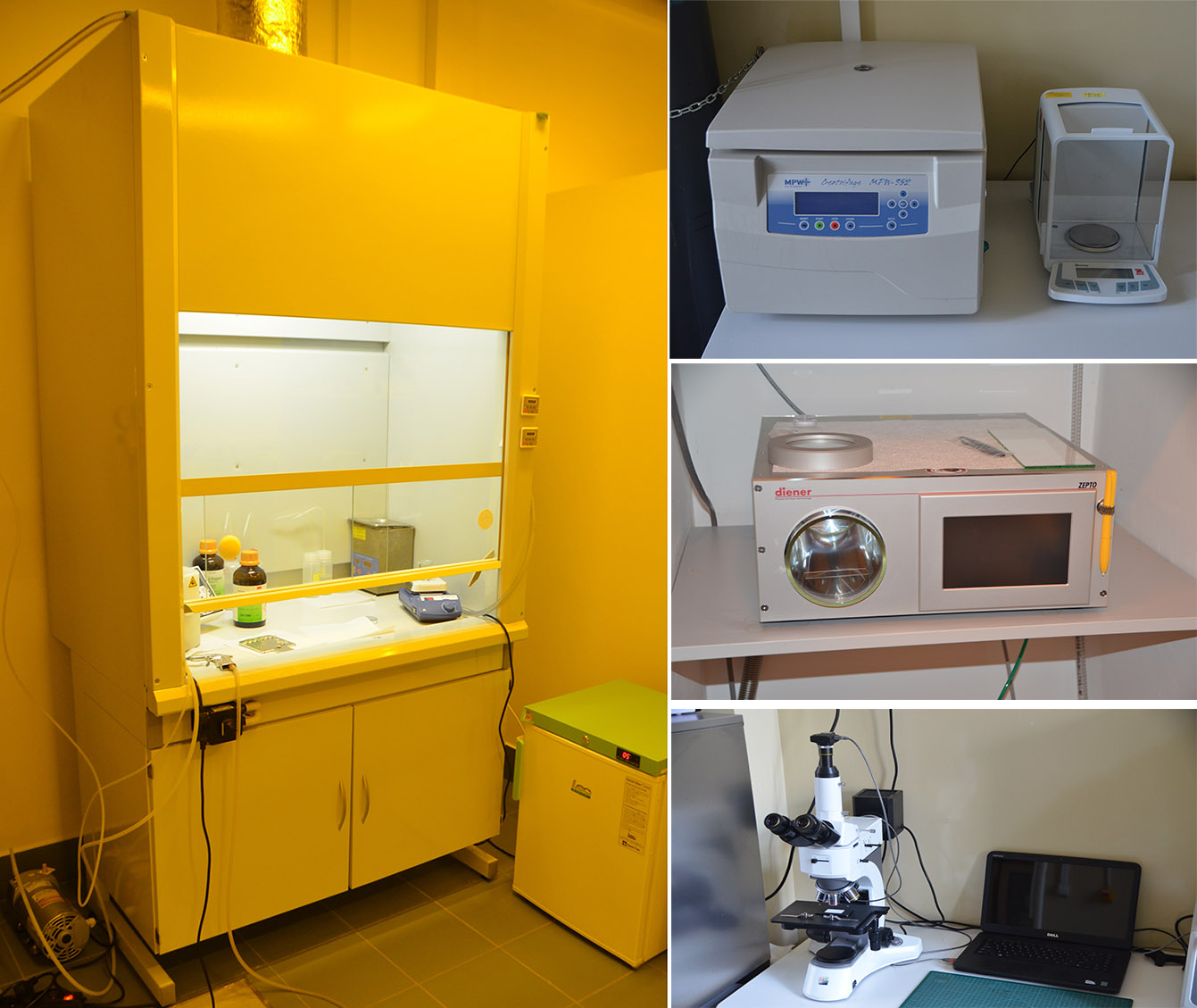
- Chemical and processing laboratory
Fully-equipped chemical laboratory suited for preparation of 2D materials and carbon nanostructures (3 fume hoods, precision scales, centrifuges, ultrasonic baths, spincoater, oxygen plasma, optical microscope with filters, annealing furnaces, vacuum filtration sets, among others)
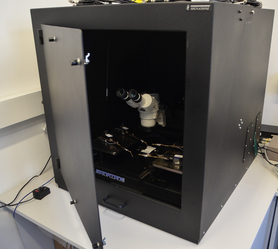
- Needle station for voltage-current characteristics measurements (Signatone)
Device adapted to measure nanodevices and at low current, 5 measurements terminals, DC & RF
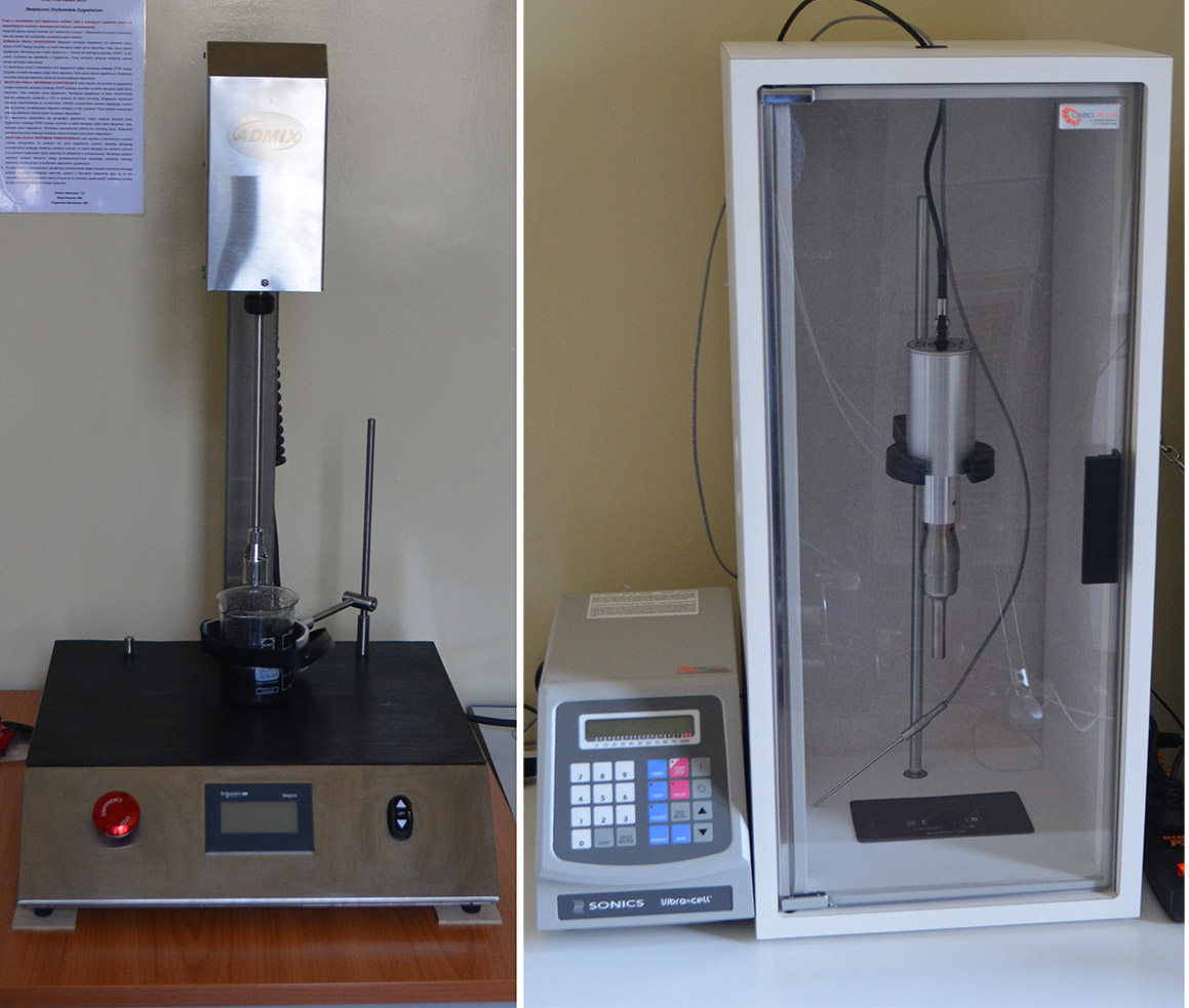
- Set of devices for wet exfoliation of 2D materials
Admix laboratory mixer (12k RPM), equipped with roto-stat and roto-solver technology. Ultrasonic homogenizer, model Vibracell 750W